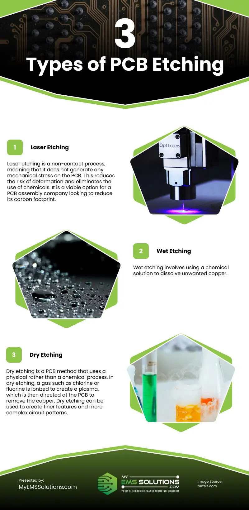
The creation of printed circuit boards depends on the complex PCB etching process. By successfully removing copper from the PCB, it aids in the production of the final circuit layout. Etching may be done anywhere, but if you’ve never done it before, the procedure might be a little challenging. This infographic explains PCB etching, including its description, kinds, and application procedures.
What Is PCB Etching?
By eliminating surplus copper from a printed circuit board (PCB), the desired circuit layout may be created. The use of a chemical solution, such as ferric chloride, is the most used method of PCB etching.
What Are the Various Kinds of Etching?
1. Laser Etching
Typically, the PCB is exposed to a concentrated laser beam that is directed at it; this eliminates copper from the PCB just where the circuit layout is to be constructed.
2. Wet etching
Unwanted copper is dissolved using a chemical solution during wet etching. The procedure can be divided into:
• Alkaline etching
Typically, the PCB is submerged in the solution during the procedure, allowing the copper to be selectively removed from the locations where the circuit layout is to be produced.
• Acidic etching
Acidic etching entails removing the copper off the PCB by employing an acidic solution, such as ferric chloride or cupric chloride.
3. Dry etching
Dry etching removes the unneeded copper from the PCB physically, using technology like plasma etching, as opposed to utilizing a liquid etchant.
How to Etch a PCB?
The steps below must be followed in order to etch a PCB:
1. Prepare the PCB:
To get rid of any debris, grease, or other impurities, carefully clean the PCB. The regions of the PCB where you want the copper to remain should then be covered with a masking substance (such as a photoresist film or liquid).
2. Select an etching method:
A dry, laser, or wet etching option is available. Use a brush or spray bottle to evenly coat the PCB’s surface if the etching procedure calls for the use of a chemical.
3. Monitor the etching procedure:
The kind of etchant used, the PCB’s thickness, and the solution’s temperature all affect how long it takes to finish the etching.
4. Wash down the PCB:
After the etching is finished, properly rinse the PCB with water to get rid of any leftover etchant solution.
5. Strip off the masking material:
To show the final PCB, take off the masking material when the PCB has dried.
6. Wipe the PCB:
Remove any remaining residue from the printed circuit board using alcohol or degreaser.
7. Perform an examination:
Verify the accuracy of the circuit pattern and the absence of any flaws or issues by inspecting the PCB.
8. Apply solder mask:
Applying a layer of solder mask helps protect the copper lines and provide insulation, however, it is not required.
Ready to etch your PCBs?
Etching can assist you in producing incredibly exact and delicate circuit layouts, whether you’re working with an EMS business or doing everything by yourself. It is also appropriate for high-volume production since it can be used to swiftly and effectively create many PCBs. Etching is significantly less costly than other ways of making circuit designs, such as wire wrapping or point-to-point assembly.
source: https://www.myemssolutions.com/pcb-etching-everything-you-need-to-know/
Comments
Download this infographic.
